(Hong Kong)

Product Summary
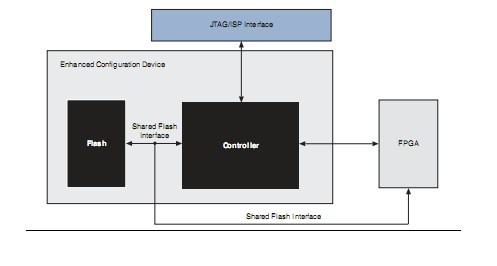
The Altera enhanced configuration device is a single-device, high-speed, advanced
configuration solution for very high-density FPGAs. The core of an enhanced
configuration device is divided into two major blocks: a configuration controller and a
flash memory. The flash memory is used to store configuration data for systems made
up of one or more Altera FPGAs. Unused portions of the flash memory can be used to
store processor code or data that can be accessed via the external flash interface after
FPGA configuration is complete. Table1–1 summarizes the features of Altera
configuration devices and the amount of configuration space they hold.
Parametrics
Flash Memory
Device Grade Package Leaded Lead-Fee
EPC4 Commercial PQFP 100 Intel (1) or Micron Intel (1) or Micron
ndustrial PQFP 100 Intel (1) or Micron Intel (1)
EPC8 Commercial/ PQFP 100 Intel (1) or Sharp Intel (1)
Industrial
EPC16 Commercial UBGA 88 Intel (1) or Sharp Intel (1) or Sharp
Industrial UBGA 88 Intel (1) or Sharp Intel (1)
Commercial/ PQFP 100 Intel (1) or Sharp Intel (1)
Industrial
Features
1. Single-chip configuration solution for Altera? ACEX? 1K, APEX? 20K (including
APEX 20K, APEX 20KC, and APEX20KE), APEX II, Arria?
GX, Cyclone?, Cyclone
II, FLEX? 10K (including FLEX10KE and FLEX10KA), Mercury?, Stratix? II, and
Stratix II GX devices
2. Contains 4-, 8-, and 16-Mbit flash memories for configuration data storage
3.On-chip decompression feature almost doubles the effective configuration
density
4. Standard flash die and a controller die combined into single stacked chip package
5. External flash interface supports parallel programming of flash and external
processor access to unused portions of memory
6. Flash memory block/sector protection capability via external flash interface
7. Supported in EPC16 and EPC4 devices
8. Page mode support for remote and local reconfiguration with up to eight
configurations for the entire system
9. Compatible with Stratix series Remote System Configuration feature
10. Supports byte-wide configuration mode fast passive parallel (FPP); 8-bit data
output per DCLK cycle
11. Supports true n-bit concurrent configuration (n = 1, 2, 4, and 8) of Altera FPGAs
12. Pin-selectable 2-ms or 100-ms power-on reset (POR) time
13. Configuration clock supports programmable input source and frequency synthesis
14. Multiple configuration clock sources supported (internal oscillator and
external clock input pin)
15. External clock source with frequencies up to 100 MHz
16. Internal oscillator defaults to 10 MHz; Programmable for higher frequencies of
33, 50, and 66 MHz
17. Clock synthesis supported via user programmable divide counter
18. Available in the 100-pin plastic quad flat pack (PQFP) and the 88-pin Ultra
FineLine BGA? (UFBGA) packages
19. Vertical migration between all devices supported in the 100-pin PQFP package
20. Supply voltage of 3.3 V (core and I/O)
21. Hardware compliant with IEEE Std. 1532 in-system programmability (ISP)
specification
22. Supports ISP via Jam Standard Test and Programming Language (STAPL)
23. Supports JTAG boundary scan
24. nINIT_CONF pin allows private JTAG instruction to start FPGA configuration
25. Internal pull-up resistor on nINIT_CONF always enabled
26. User programmable weak internal pull-up resistors on nCS and OE pins
27. Internal weak pull-up resistors on external flash interface address and control
lines, bus hold on data lines
28. Standby mode with reduced power consumption
Diagrams
| Image | Part No | Mfg | Description |  |
Pricing (USD) |
Quantity | ||||||
|---|---|---|---|---|---|---|---|---|---|---|---|---|
 |
 EP1K100QC208-3 |
|
IC ACEX 1K FPGA 100K 208-PQFP |
Data Sheet |
|
|
||||||
|
EP1K100QC208-3N |
|
IC ACEX 1K FPGA 100K 208-PQFP |
Data Sheet |
|
|
||||||