(Hong Kong)

Product Summary
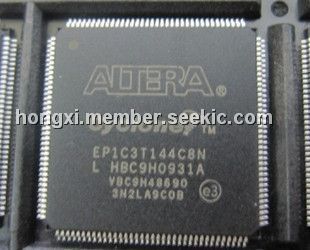
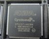
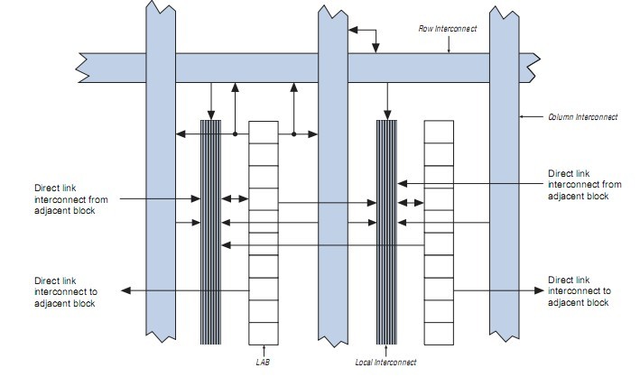
EP1C3T144 EP1C3T144C8N Cyclone devices contain a two-dimensional row- and column-based
architecture to implement custom logic. Column and row interconnects of
varying speeds provide signal interconnects between LABs and
embedded memory blocks.
EP1C3T144 EP1C3T144C8N The logic array consists of LABs, with 10 LEs in each LAB. An LE is a small
unit of logic providing efficient implementation of user logic functions.
LABs are grouped into rows and columns across the device. Cyclone
devices range between 2,910 to 20,060 LEs.
EP1C3T144 EP1C3T144C8N Cyclone devices provide a global clock network and up to two PLLs. The
global clock network consists of eight global clock lines that drive
throughout the entire device. The global clock network can provide clocks
for all resources within the device, such as IOEs, LEs, and memory blocks.
The global clock lines can also be used for control signals. Cyclone PLLs
provide general-purpose clocking with clock multiplication and phase
shifting as well as external outputs for high-speed differential I/O
support.
Parametrics
Device 100-Pin 144-Pin 240-Pin 256-Pin 324-Pin 400-Pin
TQFP (1) TQFP (1), (2) PQFP (1) FineLine BGA FineLine BGA FineLine BGA
EP1C3 65 104
Dimension 144-Pin TQFP
Pitch (mm) 0.5
Area (mm2) 484
Length × width 22 × 22
(mm × mm)
Features
1.2,910 to 20,060 LEs, see Table1
2. Up to 294,912 RAM bits (36,864 bytes)
3.Supports configuration through low-cost serial configuration device
4.Support for LVTTL, LVCMOS, SSTL-2, and SSTL-3 I/O standards
5.Support for 66-MHz, 32-bit PCI standard
6. Low speed (311 Mbps) LVDS I/O support
7.Up to two PLLs per device provide clock multiplication and phase
shifting
8.Up to eight global clock lines with six clock resources available per
logic array block (LAB) row
9. Support for external memory, including DDR SDRAM (133 MHz),
FCRAM, and single data rate (SDR) SDRAM
10.Support for multiple intellectual property (IP) cores, including
Altera? MegaCore? functions and Altera Megafunctions Partners
Program (AMPPSM) megafunctions
Diagrams
| Image | Part No | Mfg | Description |  |
Pricing (USD) |
Quantity | ||||||
|---|---|---|---|---|---|---|---|---|---|---|---|---|
 |
 EP1C3T144C8N |
|
IC CYCLONE FPGA 2910 LE 144-TQFP |
Data Sheet |
|
|
||||||
| Image | Part No | Mfg | Description | |
Pricing (USD) |
Quantity | ||||||
 |
EP1C12 |
Other |
|
Data Sheet |
Negotiable |
|
||||||
 |
EP1C12F256C6 |
|
IC CYCLONE FPGA 12K LE 256-FBGA |
Data Sheet |
|
|
||||||
|
EP1C12F256C6N |
|
IC CYCLONE FPGA 12K LE 256-FBGA |
Data Sheet |
|
|
||||||
|
EP1C12F256C7 |
|
IC CYCLONE FPGA 12K LE 256-FBGA |
Data Sheet |
|
|
||||||
|
EP1C12F256C7N |
|
IC CYCLONE FPGA 12K LE 256-FBGA |
Data Sheet |
|
|
||||||
|
EP1C12F256C8 |
|
IC CYCLONE FPGA 12K LE 256-FBGA |
Data Sheet |
|
|
||||||